Printed circuit boards (PCBs) are the backbone of modern electronics, powering everything from smartphones to industrial machinery. Custom PCBs take this further, offering tailored solutions that cater to specific needs, improving performance, and enabling innovation. But with technology advancing at lightning speed, the field of custom PCB design is evolving rapidly.
If you’re a PCB designer, electrical engineer, or tech enthusiast, this post will help you uncover some of the latest trends, explore how AI and automation are reshaping the field, and understand the challenges and opportunities ahead for the industry. Plus, we’ll also share insight into how companies like Avantari are leading the way with cutting-edge solutions.
Emerging Trends in PCB Technology
Custom PCB design is no longer limited to just creating functional boards. It’s about solving complex challenges in more efficient and creative ways. Here are some of the biggest trends transforming the landscape:
1. Flexible PCBs
Unlike traditional rigid PCBs, flexible PCBs (or Flex PCBs) bend and conform to unique shapes, opening a world of new possibilities for device designs. They are ideal for applications in wearables, medical devices, and anything requiring compact, lightweight, and durable technology.
For example:
- Wearables use Flex PCBs to fit into small, curved spaces like watch bands.
- Medical devices like pacemakers leverage their durability and reliability under dynamic conditions.
These designs not only enable creative device form factors but also improve product durability through shock resistance and better heat dissipation.
2. High-Density Interconnect (HDI) PCBs
With increasing miniaturization in electronics, HDI PCBs are at the forefront of modern design. By utilizing micro vias and thinner layers, HDI PCBs maximize component density without increasing the size of the board. This results in better signal quality, faster transmission, and higher performance.
Practical applications include:
- Mobile phones and laptops, where space efficiency and performance are paramount.
- Aerospace and automotive systems need compact and robust solutions.
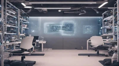
3. AI-Driven PCB Design
AI has entered the realm of PCB design in a big way. Today, advanced algorithms help designers optimize layouts, reduce signal interference, and minimize production costs. AI-powered tools are capable of analyzing complex data sets, predicting potential design flaws, and offering intelligent suggestions to achieve better outcomes.
For instance, modern AI tools can:
- Shorten the iterative design process by automating repetitive tasks like trace routing.
- Perform thermal simulations to optimize heat management.
4. User Experience Meets Hardware Design
UX/UI design is no longer confined to software. Hardware, and particularly custom PCBs, have started to prioritize the user experience embedded in physical layouts.
This UX-driven approach ensures:
- Easier maintenance by offering clear labeling for components.
- Streamlined assembly processes optimized for technicians on production lines.
By focusing on human interaction with hardware, UX/UI improvements in PCBs make them as user-centered as the products they power.
The Role of AI and Automation in PCB Development
AI and automation are revolutionizing custom PCB design by making the process faster, more cost-effective, and more accurate. Here’s how:
- Automation of Repetitive Tasks: Automated tools now handle essential but time-consuming tasks such as schematic capture, layout designs, and trace routing.
- Intelligent Design Assistance: AI algorithms analyze designs in real time, providing recommendations for improving routing efficiencies, reducing electromagnetic interference (EMI), and optimizing power delivery networks (PDNs).
- Error Reduction: Automation minimizes manual errors, identifying potential manufacturing defects or thermal issues long before production begins.
- Prototyping Revolution: Automated prototyping allows businesses to test ideas on the go, reducing time-to-market for innovations.
The rise of AI-powered CAD tools has already given designers better control and accuracy over their projects. These innovations are enabling engineers to focus on creativity rather than manually fixing errors, ultimately opening doors to groundbreaking product designs.
Challenges and Opportunities for Businesses
While the advancements in custom PCB design are promising, they also come with their share of challenges:
Challenges
- Complexity in Design: The growing demand for smaller, more complex PCBs requires enhanced expertise and tools.
- Higher Costs: Adopting state-of-the-art technologies like HDI or AI-driven tools poses upfront investment challenges.
- Environmental Regulations: Compliance with global regulations on e-waste and sustainability can complicate manufacturing processes.
Opportunities
- Mass Customization: Businesses now can create highly specialized boards for niche markets, improving product-market fit.
- Improved Efficiency: Using automation and AI reduces both time and waste, offering sizeable cost efficiencies.
- Sustainable Practices: Investing in eco-friendly materials and processes not only benefits the planet but also aligns with increasing consumer demand for sustainable products.
For businesses willing to adapt, the opportunities far outweigh the challenges. With the right investments in technology and talent, they can achieve significant ROI while driving innovation in their respective industries.
How Avantari Helps with Cutting-Edge PCB Solutions
Avantari is at the forefront of custom PCB technology, bridging the gap between creative ambition and practical execution. Here’s how we empower our clients:
- End-to-End Expertise: From schematic design to testing and mass production, Avantari provides full-stack PCB solutions tailor-made for your project.
- AI-Powered Prototyping: Our advanced design tools leverage AI for faster, smarter, and more precise iterations.
- UX-Focused Designs: By integrating UX principles into PCB layouts, we ensure maximum ease of use and compatibility for end-users.
- Sustainability Practices: Our solutions are built with compliance and eco-friendliness in mind, helping your business align with global sustainability goals.
No matter the complexity, Avantari brings your idea to life with seamless execution, backed by a team of experienced engineers and designers.
What’s Next for PCB Technology?
The future of custom PCB design lies in its ability to adapt to the fast-evolving tech landscape. From flexible materials and 3D-printed boards to edge computing and IoT integrations, the possibilities seem endless.
To designers and engineers, the message is clear: explore, experiment, and stay open to new tools and methods. And for businesses, staying ahead means partnering with innovators already paving the way for smarter, more sustainable PCB solutions.
Whether you’re looking to optimize your current PCB designs or explore futuristic concepts, Avantari is ready to help. Contact us today and take the next leap in custom PCB design!